Objective: develop the nanofabrication methods and fabricate several types of X-ray optics including zone plates, gratings, coded apertures, and others. The Optics group collaborates with various beamlines at APS and other Synchrotron facilities by providing the fabrication capabilities to support current programs and to develop new concepts. Optics are fabricated using Optics group resources and those at the Center for Nanoscale Materials (CNM). Many of the optics fabricated are characterized at 1-BM Optics and Detector testing beamline, with alternative characterization to include imaging methods such as secondary electron microscopy (SEM) or at the intended beamline instrument. These combinations of capabilities have been used to advance X-ray science and will continue to be used to develop the next generation of nano-fabricated X-ray optics. Work requests can be submitted by filling the Optics Group's work request from.
|
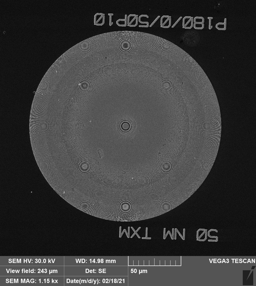
Zone Plates: The primary nanofabricated X-ray optics development project involves focusing hard X-rays for sub-100 nm focus spots. Zone plates have been deployed at various beamlines at APS with outer zone width down to 16 nm [V. De Andrade, et al., Adv. Mat. 33.21 (2021), doi: 202008653], though 30-50 nm (Figure 1) are more commonly used. Zone plate can be designed specifically for the beamline and technique.  |
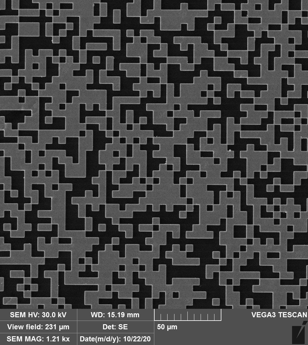
Gratings and Coded Masks: in-house development of micron sized X-ray optics has included phase gratings for interferometry and coded masks for wavefront measurements, and coded apertures for depth resolved measurements. Fabrication methods and recipes for gratings [S. Marathe, et. al., J. Visualized Exp. 116, e53025 (2016) doi: 10.3791/53025] are applicable to a wide variety of samples for X-ray optics. Coded-mask-based multi-contrast imaging (CMMI) for X-rays was developed by the Optics group [Qiao, Zhi, et al., App. Phys. Let. 119.1 (2021): doi:10.1063/5.0053553.] (Figure 2); and used for imaging and wavefront measurements. Coded apertures have been fabricated for depth-resolved Laue diffraction (Gürsoy, Doğa, et al., J. of Appl. Cryst. 55, no. 5 (2022): doi: https://doi.org/10.1107/S1600576722007099) to increase the speed acquiring data by a factor greater than five, and the optic can be used for other depth-resolved imaging methods. Most 2-D micron sized pattern is likely possible, contact staff to discuss your particular project.
|
Capabilities: The resources available and techniques developed include a wide array of materials and sample types.
|

