|
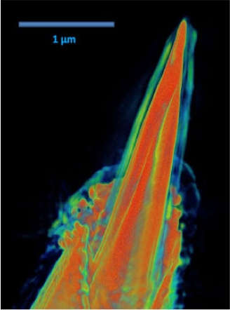
The spatial resolution in SPM depends on the sharpness of the tip. However, in SXSPM, in addition to tunneling current (STM) or force (AFM), x-ray photoabsorption can yield extra electrons that are ejected from the sample and collected at the tip. These photo-ejected electrons are generally not only detected at the apex of the tip but also at the sidewalls, which consequently will degrade spatial resolution of any measurement. Thus, “smart” tips have to be developed and utilized. The term “smart” tip refers to probes that are entirely coated by an insulating film except at the very tip apex in order to minimize the background caused by photo-ejected electrons collected through the sidewalls.
We have utilized a combination of electron beam physical vapor deposition (EBCVD) and focused ion beam (FIB) milling in order to grow “smart” tips. The SiO2 coating strongly reduces the number of photo-ejected electrons. The structural integrity of smart tips can be studied by hard x-ray nanotomography, which provides an important three-dimensional view of insulator-coated tips. The ability to see the internal structure of the coatings with x-ray nanotomography at a voxel resolution of 30 nm has helped to better understand the coating process, which in turn guarantees exceptionally performing tips for SXSPM research.
The development of insulator-coated tips with ultra-small conducting apex is indispensible for advances in synchrotron-based scanning probe microscopy, which has the potential to provide nanoscale imaging and spectroscopy with chemical, electronic, and magnetic contrast.
Back to Research | Next
|
|
|