
|
|
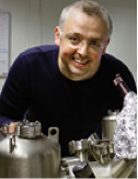
Prof Anders Mikkelsen from Lund University in Sweden is well known for his development of groundbreaking tools and concepts to allow imaging inside, onside and topside of semiconductor nanowires down to the single atom level using scanning tunneling microscopy (STM). His research has also involved a broad range of materials such as semiconductors, metal alloys, oxides, quasi crystals, water overlayers and magnetic materials. On June 11, he presented a seminar entitled "Direct imaging of nanostructure surfaces and interfaces to the atomic scale using both scanning probe and synchrotron light based microscopy". In this well-received talk he covered his recent STM work on nanowires as well as the status of NanoMAX, an imaging beamline at the Swedish synchrotron radiation source MAX IV. |