| Techniques | Coherent X-ray surface imaging, grazing incidence X-ray scattering |
| Photon beam energy | 6-25 keV |
| X-ray spot size | 0.6x0.35 to 3.5 x 1.7 µm2(HxV) |
| Working distance | 2.9 to 21.8 m |

A lot of power can exist on the surface of things, from an energy-generating perspective.
Consider solar panels. They deliver a big energy punch despite their flyweight demand on the environment. They rely on very thin films of photovoltaic cells to form a surface that converts sunlight into electricity. In a similar way, silicon chips inside nearly all small electronic devices (such as those that power processors or cameras inside cell phones) use fine layered stacks of integrated circuits to store hundreds of gigabytes or terabytes of memory.
Scientists would like to know more about what is happening within each of these extremely thin layers, most typically thinner than one thousandth the diameter of a single human hair. The ability to see at which layer a failure is likely or imminent will improve engineers’ ability to address potential problems and come up with better overall designs. Energy efficiency and operational speed can be improved with more precise insights.

The Coherent Surface Scattering Image (CSSI) beamline at 9-ID of the upgraded Advanced Photon Source (APS) will help scientists study fine layers such as these, as well as other thin stacks of material used for various valuable purposes. The CSSI beamline will enable better visualization of nano-to-millimeter-sized structures over time and in 3D, and it will potentially lead to the development of superior materials and polymers capable of powering devices with greater energy efficiency.
Instead of seeing a sample directly, as one would do through a microscope, CSSI enables researchers to use a laser-like coherent and bright X-ray beam to create an image of the 3D volume of a thin film at a surface or interface using reflected scattering data. The data contains information of all structures of the sample and can be reconstructed into a visualization resembling real space.

By showing even more clearly things happening at the nanometer level of a structure, CSSI users should be able to improve their understanding of different phases of various additive manufacturing processes. They can also conduct better experiments for medical imaging sensors, single electron transistors, photovoltaics, and quantum dots, which are important to the pursuit of quantum computing. As the design of materials trends toward ever smaller and thinner membranes, layers and stacks, scientists will use CSSI to examine reflected scattering images to reconstruct patterns and iterations within a few nanometers of resolution.
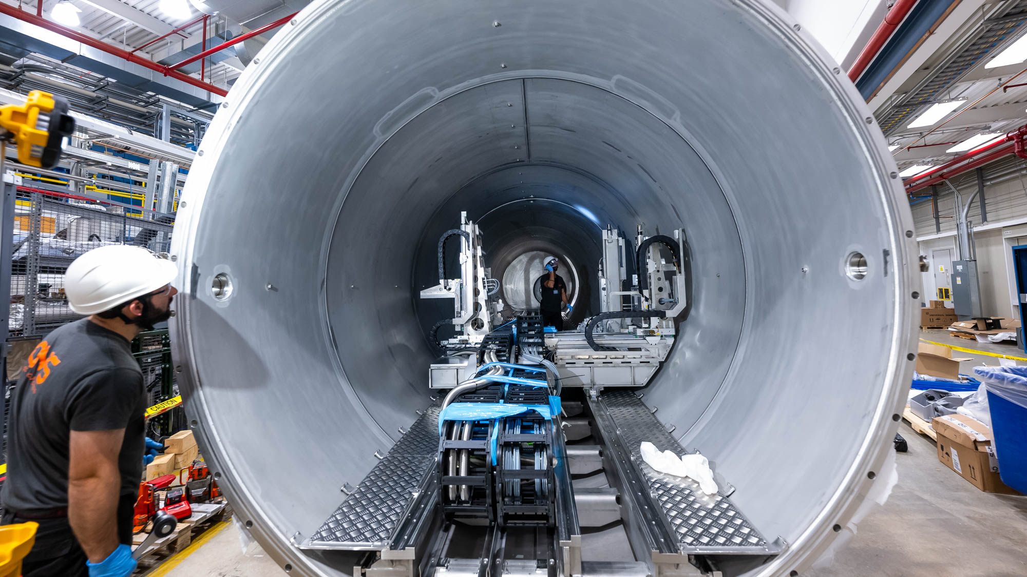
CSSI’s giant vacuum chamber is a landmark of the upgraded APS. Its design includes the “Grand Tube,” a 66-foot-long stainless-steel vacuum tube approximately nine feet in diameter.
In the Grand Tube, large-scale mobile X-ray detectors collect the scattering images from the samples. The detectors move in all three dimensions, back and forth, left and right and up and down within the tube, allowing scattering images to be collected from multiple directions. This will present new views of reflections from different surfaces and interfaces, which scientists can then photograph and reconstruct into 3D images to better visualize the geometry of structures.
BEAMLINE CONTACT:
Jin Wang,wangj@aps.anl.gov
