
Over the past three decades, scanning tunneling microscopy (STM) has rapidly become a major component of the condensed matter physics toolbox. While STM can provide vast quantities of data about the electronic, structural, and magnetic properties of materials at atomic resolution, its Achilles heel is its inability to characterize elemental species. But a team from Argonne National Laboratory and Ohio University has found a way around this limitation by combining STM with the spectroscopic versatility of synchrotron x-rays, achieving chemical fingerprinting of individual nickel clusters on a copper surface at a resolution of 2 nm, creating a powerful and versatile nanoscale imaging tool with exciting promise and potential for the materials and biological sciences. Their work was published in Nano Letters.
Working at the Center for Nanoscale Materials (CNM)/X-ray Science Division 26-ID beamline of the U.S. Department of Energy’s Advanced Photon Source, the researchers took advantage of some new technological innovations developed by Argonne researchers.
However, the team had to overcome some experimental hurdles to combine STM with synchrotron x-rays. The resolution and sensitivity of STM can be adversely affected by photoejected electrons from the sample interfering with the measurement of tunneling effects.
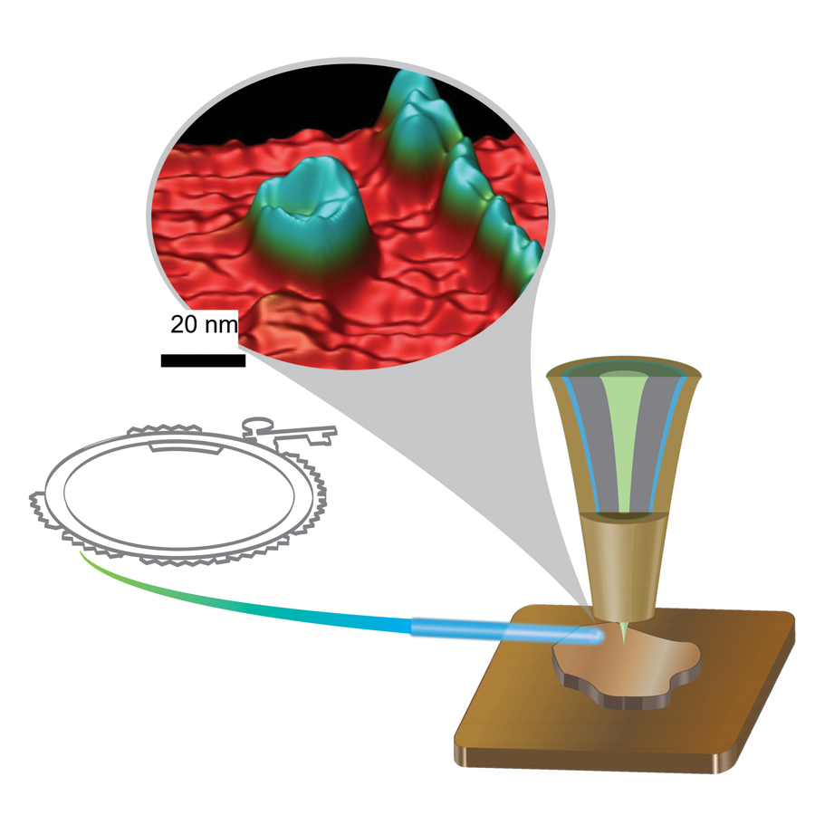
The Argonne researchers invented and patented a nanofabricated “smart tip” for the scanning tunneling microscope that sharply focuses detection of electrons solely to those collected at the scanning tip where it interacts with the sample, ignoring the background electrons from the sidewalls of the tip. The various coatings for the smart tip were grown at the CNM, and then the tip apex was exposed via focused ion beam milling carried out at the CNM Electron Microscopy Center (EMC). (The APS, CNM, and EMC at Argonne are Office of Science user facilities.)
The team also developed a filter circuit that separates the chemical and magnetic data from the x-ray-induced currents and topographical data from conventional tunneling effects into two channels, allowing them to be recorded separately without mutual interference.
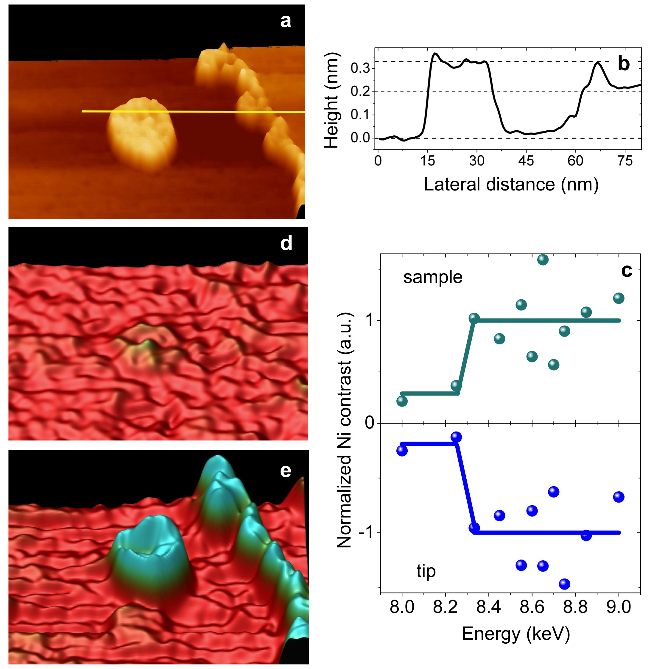
Using the markedly enhanced resolution and sensitivity made possible with these advances in synchrotron x-ray tunneling microscopy (SX-STM), the Argonne/Ohio University experiment team analyzed nickel clusters deposited on a copper surface. Usually, because chemical fingerprinting using x-rays is based on photoionization cross sections, such measurements are averaged over a rather wide surface area and depth. But the new technique was able to image and obtain a photoionization cross section of a single nickel cluster on the sample surface with 2-nm resolution.
“We have demonstrated a world record in the spatial resolution of chemical imaging using synchrotron x-ray scanning tunneling microscopy,” said Saw-Wai Hla, a co-author of the Nano Letters article.
“This has a tremendous impact for many scientific areas including materials science, chemistry, and energy materials,” said co-author Volker Rose.
Both that remarkable resolution and the precise chemical fingerprinting of individual nickel nanoclusters were also clearly evident in the topographic images of the sample surface, even down to the height of a single atom. The experimenters note that the thickness of individual clusters appears to have no effect on the contrast intensity of their chemical signature. They suggest that because tunneling is a local effect sensitive only to the topmost layer of materials, this phenomenon as observed topographically results from the tunneling of x-ray excited photoelectrons from states between the Fermi level and the work function.
While the current experiments were conducted at room temperature, the researchers anticipate achieving even better resolution in SX-STM at far lower temperatures.
Even in its present form, the techniques demonstrated here can revolutionize nanoscale imaging in realms far beyond materials science, including electronics and biology. By overcoming the inherent limitations of both STM and x-ray microscopy, this new work has also combined the strengths of each to create a powerful and versatile imaging tool with an exciting promise and potential.
— Mark Wolverton
See: Nozomi Shirato1, Marvin Cummings1, Heath Kersell2, Yang Li2, Benjamin Stripe1, Daniel Rosenmann1, Saw-Wai Hla1,2**, and Volker Rose1*, “Elemental Fingerprinting of Materials with Sensitivity at the Atomic Limit,” Nano Lett., Article ASAP (2014). DOI: 10.1021/nl5030613
Author affiliations: 1Argonne National Laboratory, 2Ohio University
Correspondence: * vrose@anl.gov, ** shla@anl.gov
This work was funded by the Office of Science Early Career Research Program through the Division of Scientific User Facilities, Basic Energy Sciences, U.S. Department of Energy, through Grant SC70705. Work at the Advanced Photon Source, the Center for Nanoscale Materials, and the Electron Microscopy Center was supported by the U.S. Department of Energy, Office of Science, Basic Energy Sciences, under Contract DE-AC02-06CH11357. H.K. and Y.L acknowledge the support by the U.S. Department of Energy, Office of Science, Basic Energy Sciences Grant DE-FG02- 02ER46012.
Argonne National Laboratory is supported by the Office of Science of the U.S. Department of Energy. The Office of Science is the single largest supporter of basic research in the physical sciences in the United States, and is working to address some of the most pressing challenges of our time. For more information, please visit science.energy.gov.