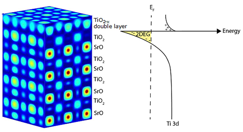
In the research field of complex oxides―materials comprised of oxygen and typically two other elements―strontium titanate (SrTiO3) has long been considered a reliable workhorse with a surface structure that can be controlled down to the atomic level. This precise level of control allows thin-film heterostructures to be grown on SrTiO3 to create atomically specific heterointerfaces. However, although the surface structure of SrTiO3 has long been considered consistent and dependable, its properties have been hard to explain. For example, although bulk SrTiO3 behaves as an insulator, unexpected properties such as high conductivity can arise at the surface. This particular property has been linked to mobile electrons confined to two dimensions (2-D), a phenomenon known as a 2-D electron gas (2DEG). However, the origins of this 2DEG were unknown. To better understand the unusual properties of SrTiO3, a team of researchers used the U.S. Department of Energy’s Advanced Photon Source (APS) to perform a variety of studies using an array of synchrotron analytical techniques on thin films of this material, both during and after synthesis. Their findings solve long-held mysteries about SrTiO3 and could lead to new ways to harness its strange properties.
To study the surface of SrTiO3 (001) both before, during, and after monolayer growth, the researchers from the Argonne National Laboratory Materials Science and X-ray Science (XSD) divisions used a molecular beam epitaxy (MBE) chamber located at the XSD Surface Scattering & Microdiffraction Group’s 33-ID-E beamline at the APS, an Office of Science user facility at Argonne, to perform in situ surface x-ray diffraction. They saw that the initial SrTiO3 surface consisted of two consecutive atomic layers of TiO2―i.e., a TiO2 double layer―rather than the expected single layer. After transporting SrTiO3 from the 33-ID-E beamline to the XSD Magnetic Materials Group’s Intermediate Energy X-ray 29-ID-C beamline at the APS in a vacuum suitcase, the researchers were able to study the surface with other analytical techniques, including x-ray photoelectron spectroscopy, x-ray absorption spectroscopy, and angle-resolved photoemission spectroscopy (ARPES). These measurements showed that the 2DEG exists at the TiO2 double layer surface.
After returning to the MBE chamber at 33-ID-E, the researchers grew one atomic plane of SrO on top of the SrTiO3 crystal. While this should have resulted in SrO at the surface, x-ray diffraction showed that the SrO monolayer diffused into the middle of the TiO2 double layer, leaving an upper surface mainly composed of TiO2. Subsequent ARPES measurements at 29-ID-C showed that the 2DEG disappeared.
Further depositions of TiO2 and SrO and further x-ray measurements revealed the ultimate source of the 2DEG: the TiO2 double layer. Although the SrTiO3 surface had long been considered to be a “perfect” surface, the synchrotron x-ray techniques showed that the TiO2 adlayer had a significant number of oxygen vacancies―areas in which oxygen atoms are missing. The defects in this adlayer create free electrons at the surface, prompting the 2DEG to form.
The researchers note that the combination of techniques they used, which probed both the physical and electronic structure of SrTiO3, were pivotal for making these findings. In the future, researchers may be able to harness the unique qualities of SrTiO3’s insulating interior and conducting surface for applications that studies have only begun to explore, such as chemically or electrically “drawing” and erasing 2DEG devices, suggesting the possibility of reconfigurable, re-purposable, and even flexible oxide electronics. Scientists may also be able to control the amount of oxygen vacancies, consequently tuning SrTiO3’s electronic properties.
The more researchers understand about this unusual material, the closer they will be to designing and deliberately creating specific interfaces for an array of unique electronic, magnetic, and optoelectronic functionalities. ― Christen Brownlee
See: Xi Yan, Friederike Wrobel, I-Cheng Tung, Hua Zhou**, Hawoong Hong, Fanny Rodolakis, Anand Bhattacharya, Jessica L. McChesney***, and Dillon D. Fong*, “Origin of the 2D Electron Gas at the SrTiO3 Surface,” Adv. Mater. 34, 2200866 (2022). DOI: 10.1002/adma.202200866
Author affiliation: Argonne National Laboratory
Correspondence: * fong@anl.gov, ** hzhou@anl.gov; *** jmcchesn@anl.gov
Research was supported by U.S. Department of Energy, Office of Science, Office of Basic Energy Sciences, Materials Sciences and Engineering Division. Use of the Advanced Photon Source, an Office of Science user facility, was supported by the U.S. Department of Energy, Office of Science, Office of Basic Energy Sciences, under Contract No. DE-AC02- 06CH11357.
The U.S. Department of Energy's APS at Argonne National Laboratory is one of the world’s most productive x-ray light source facilities. Each year, the APS provides high-brightness x-ray beams to a diverse community of more than 5,000 researchers in materials science, chemistry, condensed matter physics, the life and environmental sciences, and applied research. Researchers using the APS produce over 2,000 publications each year detailing impactful discoveries, and solve more vital biological protein structures than users of any other x-ray light source research facility. APS x-rays are ideally suited for explorations of materials and biological structures; elemental distribution; chemical, magnetic, electronic states; and a wide range of technologically important engineering systems from batteries to fuel injector sprays, all of which are the foundations of our nation’s economic, technological, and physical well-being.
Argonne National Laboratory seeks solutions to pressing national problems in science and technology. The nation's first national laboratory, Argonne conducts leading-edge basic and applied scientific research in virtually every scientific discipline. Argonne researchers work closely with researchers from hundreds of companies, universities, and federal, state and municipal agencies to help them solve their specific problems, advance America's scientific leadership and prepare the nation for a better future. With employees from more than 60 nations, Argonne is managed by UChicago Argonne, LLC, for the U.S. DOE Office of Science.
The U.S. Department of Energy's Office of Science is the single largest supporter of basic research in the physical sciences in the United States and is working to address some of the most pressing challenges of our time. For more information, visit the Office of Science website.
