Complex oxides are compounds that contain oxygen and at least two other elements. These materials exhibit the unusual electric and magnetic properties needed for next-generation electronic devices. Because silicon is the dominant electronic material, any promising complex oxide should be capable of interfacing with it. However, achieving this interface is challenging. For instance, lead zirconium titanate (PZT) is a well-known complex oxide that is strongly ferroelectric, but it fails to properly “grow” on silicon. One solution is to form thin-film PZT on a compatible substrate and then transfer it to silicon. While conceptually straightforward, the effects of such transfers on thin films are largely unknown. In order to resolve this mystery a research team investigated the properties of a transferred thin film using several techniques, including scanning probe microscopy and charge-voltage relationship measurement performed at Argonne National Laboratory's Material Science Division (MSD), and x-ray nanodiffraction experimentation carried out at the U.S. Department of Energy’s Advanced Photon Source (APS) and Center for Nanoscale Materials (CNM), also at Argonne. The researchers found that the static ferroelectric surface charge and structural properties of the transferred PZT film were more-or-less preserved. However, the ferroelectric’s dynamic electromechanical response changed substantially. Taken together, these findings, published in the journal Advanced Materials, demonstrate the feasibility of transferring thin-film PZT and other complex oxides to silicon, thereby promoting their use for applications including non-volatile computer memory and quantum computing.
PZT was developed in the 1950s as a piezoelectric compound, meaning it produces electricity when deformed, and changes shape in response to an electric field. Due to its excellent piezoelectric properties, PZT is widely used in ultrasound transducers and actuators. This widely-used material is also ferroelectric, meaning that positive and negative charge separation spontaneously arises. Interest in ferroelectrics has increased due to their potential use in computational, switching, and sensor applications. But the advantages offered by ferroelectrics depend upon integration with silicon. Due to their mismatched crystalline structures, PZT will not correctly form on silicon. Fortunately, the lead author of this work previously (while doing postdoctoral research at UC Berkeley) developed an alternative approach known as layer transfer technique (LTT). Using LTT allows scientists to form a thin-film complex oxide on a highly-compatible substrate and then transfer the film to another substrate.
For this study, the researchers from Argonne, the Korea Advanced Institute of Science and Technology (KAIST), and the University of California, Berkeley used pulsed laser deposition to form a crystalline layer of PZT on one substrate and then moved it to another substrate. The researchers were interested in resolving several issues, including whether LTT could transfer a PZT film without destroying it; to provide the first-ever look at the underside of a complex oxide thin-film; and to determine how the transfer affected the film's properties.
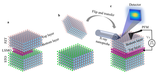
Figure 1 illustrates the experimental concept. Thin-film PZT (Fig. 1a) is extracted from the substrate (Fig. 1b) and placed upside-down on a similar substrate (Fig. 1c). This LTT procedure, performed in the CNM cleanroom facility, releases the molecular bonds between the PZT and its original substrate, resulting in a freestanding film resting on the second substrate. Scanning probe microscopy experiments and charge-voltage relationship measurement, performed at MSD, revealed drastically reduced dynamic ferroelectric properties in freestanding film. X-ray nanoprobe data, gathered at the joint CNM/X-ray Science Division 26-ID beamline at the APS, confirmed that the transferred film's crystalline structure remained intact.

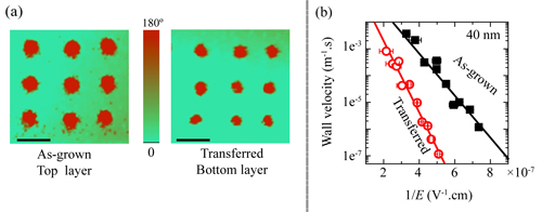
Polarized regions are created using scanning probe microscope in ferroelectric films. The nanoscale spaces between two oppositely-polarized areas are called domain walls. Upon applying an electric field, the intervening domain walls can rapidly shift. Taking snapshots of the position of a particular domain wall after applying pulsed electric fields revealed that domain wall movement was 100 to 1000 times slower in the freestanding film versus the originally-deposited form (Fig. 2a). The reduction of domain wall speed was unexpected since theory indicated this speed should actually increase in a strain-free, freestanding film. The researchers attributed the dramatic reduction in wall speed to the induced flexoelectric fields within the film that altered its polarization landscape. The presence of such flexoelectric fields was confirmed by capacitance measurements and numerical simulations. The induced flexoelectric field arose from the pronounced crystallographic tilts caused by thin-film separation, as revealed by the contact mode scanning probe microscopy and x-ray data.
Although wall speed was lowered in the freestanding film, its polarization strength was little changed. The fact that the crystallographic structure and important ferroelectric properties (polarization strength, etc.) were largely preserved in the freestanding PZT film indicates that integrating thin films of complex oxides with silicon is entirely feasible using LTT. However, the researchers note that effects arising from the flexoelectric fields will require additional investigation. ― Philip Koth
See: Saidur R. Bakaul1*, Jaegyu Kim2, Seungbum Hong2, Mathew J. Cherukara1, Tao Zhou1, Liliana Stan1, Claudy R. Serrao3, Sayeef Salahuddin3, Amanda K. Petford-Long1, Dillon D. Fong1, and Martin V. Holt1, “Ferroelectric Domain Wall Motion in Freestanding Single-Crystal Complex Oxide Thin Film,” Adv. Mater. 32, 1907036 (2020). DOI: 10.1002/adma.201907036
Author affiliations: 1Argonne National Laboratory, 2Korea Advanced Institute of Science and Technology (KAIST), 3University of California, Berkeley
Correspondence: *sbakaul@anl.gov
Scanning probe microscopy, electronic transport, and sample fabrication carried out at Argonne National Laboratory were supported by the U.S. Department of Energy (DOE) Office of Science-Basic Energy Sciences, Materials Sciences and Engineering Division. Use of the Center for Nanoscale Materials was supported by the U.S. DOE Office of Science-Basic Energy Sciences, under contract No. DE-AC02- 06CH11357. Materials growth carried out at the University of California Berkeley was supported by Office of Naval Research Contract No: N00014-14-1-0654. J.K. and S.H. acknowledge support from Brain Korea 21 Plus and KAIST. This research used resources of the Advanced Photon Source, a U.S. DOE Office of Science User Facility operated for the DOE Office of Science by Argonne National Laboratory under Contract No. DE-AC02-06CH11357.
The U.S. Department of Energy's (DOE) APS is one of the world’s most productive x-ray light source facilities. Each year, the APS provides high-brightness x-ray beams to a diverse community of more than 5,000 researchers in materials science, chemistry, condensed matter physics, the life and environmental sciences, and applied research. Researchers using the APS produce over 2,000 publications each year detailing impactful discoveries, and solve more vital biological protein structures than users of any other x-ray light source research facility. APS x-rays are ideally suited for explorations of materials and biological structures; elemental distribution; chemical, magnetic, electronic states; and a wide range of technologically important engineering systems from batteries to fuel injector sprays, all of which are the foundations of our nation’s economic, technological, and physical well-being.
The Center for Nanoscale Materials is one of the five DOE Nanoscale Science Research Centers, premier national user facilities for interdisciplinary research at the nanoscale supported by the DOE Office of Science. Together the NSRCs comprise a suite of complementary facilities that provide researchers with state-of-the-art capabilities to fabricate, process, characterize and model nanoscale materials, and constitute the largest infrastructure investment of the National Nanotechnology Initiative. The NSRCs are located at DOE’s Argonne, Brookhaven, Lawrence Berkeley, Oak Ridge, Sandia and Los Alamos National Laboratories. For more information about the DOE NSRCs, please visit https://science.osti.gov/User-Facilities/User-Facilities-at-a-Glance.
Argonne National Laboratory seeks solutions to pressing national problems in science and technology. The nation's first national laboratory, Argonne conducts leading-edge basic and applied scientific research in virtually every scientific discipline. Argonne researchers work closely with researchers from hundreds of companies, universities, and federal, state and municipal agencies to help them solve their specific problems, advance America's scientific leadership and prepare the nation for a better future. With employees from more than 60 nations, Argonne is managed by UChicago Argonne, LLC, for the U.S. DOE Office of Science.
The U.S. Department of Energy's Office of Science is the single largest supporter of basic research in the physical sciences in the United States and is working to address some of the most pressing challenges of our time. For more information, visit the Office of Science website.
