
The original “Nebraska Today” article by Scott Schrage can be read here.
Preparing the perfect nanoscale sandwich from oxygen-based ingredients was no picnic. But, with the assistance of the U.S. Department of Energy’s Advanced Photon Source (APS), an international team of researchers has finally managed it — ending a nearly 15-year quest to observe a phenomenon that could help power and miniaturize a future generation of electronics.
In 2004, researchers observed a gas of electrons coursing two-dimensionally through a nano-sandwich made from oxides: chemical compounds containing oxygen atoms. That demonstration of atwo-dimensional (2-D) electron gas signaled the promise of confining electric current to smaller spaces and, in turn, shrinking electronic components to smaller scales.
Yet the negatively charged electron has a counterpart – a positively charged “hole” it leaves behind when ejecting from its orbit around an atom. So physicists set out to create and observe a 2-D hole gas that likewise acts as a source of electric current.
As detailed in the journal Nature Materials, researchers from the University of Wisconsin-Madison the University of Nebraska-Lincoln, Sungkyunkwan University (South Korea), The Ohio State University, Argonne National Laboratory, and the Pohang University of Science and Technology (South Korea) accomplished the long-sought feat. Doing so required several years of perfecting both the ingredients and preparation. Nebraska’s Evgeny Tsymbal and Tula Paudel informed the latter by running theory-grounded calculations and modeling through the university’s Holland Computing Center.
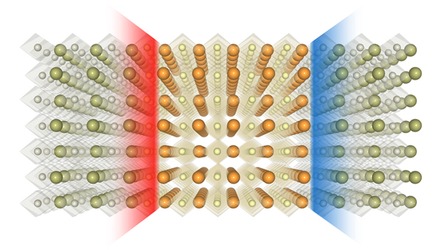
The recipe itself seemed simple enough. To produce a 2-D electron gas, researchers had previously stacked a positively charged oxide layer on a neutral base, finding that negatively charged electrons flocked downward to the nanoscopic space between the two. By adding a negatively charged layer atop the positive slice, then capping the nano-sandwich with another neutral layer, researchers had hoped to see positively charged holes mimic that behavior by migrating upward to form their own 2-D gas.
They resisted. Why? Oxygen atoms were abandoning their posts, and their positively charged vacancies — useless for producing an electric current — prevented the holes from moving on up.
“We looked at the different concentrations of the oxygen vacancies, the different positions of these defects, and how the behavior changes (as a result),” said Tsymbal, George Holmes University Professor of Physics and Astronomy.
The team found that it could get away with a few absentee oxygen atoms so long as those in the thick of the action managed to hold steady.
“Positioning is important,” said Paudel, a research assistant professor who performed most of the calculations. “You don’t want the oxygen vacancies near the region where you’re supposed to have a two-dimensional hole gas.”
Those insights, combined with precise specifications for the thickness of each slice in the nano-sandwich, guided experiments taking place at Wisconsin. By building those slices atom by atom — easier done with oxides than many other classes of materials — and fabricating the material in a pressurized, oxygen-rich environment that minimized vacancies, the Wisconsin researchers succeeded in producing and characterizing the 2-D hole gas. To verify the atomic structure of the samples, synchrotron x-ray crystal truncation rod (CTR) measurements were performed, and subsequently analyzed by the coherent Bragg rod analysis (COBRA) method. The CTR measurements were performed using an x-ray energy of 20 keV at the X-ray Science Division 12-ID-C,D beamline of the APS, which is an Office of Science user facility at Argonne.
For decades, engineers have fabricated the majority of electronic components from semiconducting materials such as silicon, the industry’s workhorse.
“The problem is that we are approaching fundamental limits,” said Tsymbal. “At some point (soon), we’ll approach certain limits beyond which we cannot continue (following) the semiconductor road map in the way that we did before. So we need to conceptually change the way our devices operate.”
One of those limits is space. The race to cram more functionality — memory, for instance — into tinier and tinier devices has left engineers looking toward oxides and other materials that, when combined, can squeeze conductivity into the tightest of confines. The new study took advantage of an oxide called strontium titanate — what Tsymbal described as the “silicon of oxide electronics” — to achieve this.
“The advantage here is that the confinement — the thickness of this two-dimensional electron or hole gas — is much smaller compared to what you have in semiconductors,” Tsymbal said. “Instead of, for example, tens of nanometers, we can confine it to one nanometer. So, in principle, we can make the devices much smaller as compared to those in semiconductor electronics.”
Though strontium titanate and its oxide brethren don’t generally exhibit magnetism on their own, they sometimes do when combined. They even show the potential for superconductivity — electric current that flows without any resistance — and other properties appealing to electric and computer engineers. As theoreticians, Tsymbal and Paudel are interested in the phenomena that could emerge from 2-D electron and hole gases flowing in parallel through the same material. Among them: the pairing of electrons and holes into particle-like excitons that behave differently as a large collective than they do alone.
“Oxides boasting these complementary 2-D gases might now begin serving as nanoscopic laboratories in which to create and study new physics,” Paudel said.
How those phenomena might eventually be applied remains an open question, Tsymbal said, but one well worth exploring.
“When researchers started working on semiconductors more than 60 years ago, nobody knew that they would become central to modern technology,” Tsymbal said. “At this point, oxide electronics are on the level of fundamental research, so it’s hard to predict where they will go.
“But you can control oxide interfaces with extreme precision. Once you have that, you can do something similar to what semiconductors achieve — but maybe also something else.”
See: H. Lee1, N. Campbell1, J. Lee2, T.J. Asel3, T.R. Paudel4, H. Zhou5, J.W. Lee1, B. Noesges3, J. Seo2, B. Park2,6, L.J. Brillson3, S.H. Oh2, E.Y. Tsymbal4, M.S. Rzchowski2, and C.B. Eom1*, “Direct observation of a two-dimensional hole gas at oxide interfaces,” Nat. Mater. 17, 231 (March 2018). DOI: 10.1038/s41563-017-0002-4
Author affiliations: 1University of Wisconsin-Madison, 2Sungkyunkwan University, 3The Ohio State University, 4University of Nebraska-Lincoln, 5Argonne National Laboratory, 6Pohang University of Science and Technology
Correspondence: *eom@engr.wisc.edu
This work was supported by the National Science Foundation (NSF) under DMREF Grant number DMR-1629270, AFOSR under award number FA9550-15-1-0334, and AOARD under award number FA2386-15-1-4046. Transport measurement at the University of Wisconsin-Madison was supported by the U.S. Department of Energy (DOE) Office of Science-Basic Energy Sciences, under award number DEFG02- 06ER46327. Research at the University of Nebraska-Lincoln was supported by the NSF MRSEC (Grant no. DMR-1420645). T.J.A. and L.J.B. acknowledge support from NSF grant DMR 1305193. STEM and in-line electron holography works by S.H.O. were supported by the Creative Materials Discovery Program through the National Research Foundation of Korea (NRF) funded by the Ministry of Science, ICT and Future Planning (NRF-2015M3D1A1070672) and NRF grant funded by the Korea government (NRF- 2015R1A2A2A01007904). This research used resources of the Advanced Photon Source, a U.S. Department of Energy (DOE) Office of Science User Facility operated for the U.S. DOE Office of Science by Argonne National Laboratory under Contract No. DE-AC02-06CH11357.
Argonne National Laboratory seeks solutions to pressing national problems in science and technology. The nation's first national laboratory, Argonne conducts leading-edge basic and applied scientific research in virtually every scientific discipline. Argonne researchers work closely with researchers from hundreds of companies, universities, and federal, state and municipal agencies to help them solve their specific problems, advance America's scientific leadership and prepare the nation for a better future. With employees from more than 60 nations, Argonne is managed by UChicago Argonne, LLC for the U.S. Department of Energy's Office of Science.
The U.S. Department of Energy's Office of Science is the single largest supporter of basic research in the physical sciences in the United States and is working to address some of the most pressing challenges of our time. For more information, visit the Office of Science website.