
 Retrieving phase information from hard (high-energy) x-ray diffraction patterns is one way to improve sample imaging. One such phase-retrieval technique uses multiple overlapping diffraction patterns derived from a coherent x-ray beam. Using this scheme, highly detailed three-dimensional (3-D) images of a sample's nanostructure have been obtained, along with additional information such as variations in the local strain field. However, phase-retrieval techniques face certain limitations, such as the need to rotate the sample. In this study, researchers implemented a new phase-retrieval technique called 3-D Bragg projection ptychography (3DBPP). A major advantage of this method is that the sample remains fixed. Utilizing a specially tailored micro-electronic prototype device, the researchers used the 3DBPP technique to create a nanoscale 3-D reconstruction of the device's lattice distortions, thereby revealing its internal strains. Employing the highly intense and coherent x-rays of the U.S. Department of Energy’s Advanced Photon Source (APS) was essential to the experiment. The comparative simplicity of 3DBPP, coupled with its powerful 3-D imaging and strain field capabilities, is expected to find application in a wide variety of experimental settings for improved 3-D x-ray microscopy of crystalline materials.
An x-ray beam interacting with a crystalline structure forms a diffraction pattern containing diverse fringes. X-ray detectors only capture part of the information in a diffraction pattern since they register only the intensity (brightness) of the diffracted x-rays and not their phase. Coherent x-rays (the type used in this study) are in-phase, meaning that the crests and valleys of the sinusoidal waves are in sync when they arrive at the sample. After diffraction from an object, however, the x-rays are perturbed and form a distinctive pattern in intensity and phase that encodes structural information about the sample. Determining how the phases of the diffracted x-rays have been shifted from their original phase is known as the “phase problem.”
It was only in the 1930s that a solution to the phase problem was devised, albeit for the optical microscope. Solving the phase problem for x-ray diffraction awaited the development of several key technologies, including x-ray mirrors and diffraction gratings; highly sensitive electronic x-ray detectors; powerful computers and algorithms for x-ray data processing; and coherent x-rays produced by synchrotron facilities like the APS.
Scientists have applied these technological advances to successfully resolve the x-ray phase problem from progressively complicated samples by gleaning information from multiple overlapping diffraction patterns. This process is known as ptychography, which exploits the presence of spatial overlap in the coherent x-ray diffraction patterns to form high-resolution 3-D images. Using these techniques, nanoscale imaging of crystalline lattices and their distortions has been achieved at length scales smaller than the size of the beam.
In relation to crystalline diffraction, current ptychography methods are hindered by the need for multiple x-ray beam diffraction angles, which is usually achieved by rotating the sample. In contrast, the 3DBPP technique relies solely on a “raster” approach wherein the beam moves laterally across the sample in a step-by-step process. The orientation of the beam (measuring a mere 46 nanometers across in this study) remains fixed relative to the sample.
Sweeping the x-ray beam across the sample yields overlapping diffraction patterns. 3DBPP utilizes back projection of the two-dimensional (2-D) structural information contained in each of these diffraction patterns. Taken together, the back projections of hundreds of 2-D diffraction patterns are utilized to produce a 3-D image that is sensitive to lattice strain in the crystal. 3DBPP takes advantage of this fact and integrates it into phase retrieval so that both the phase problem and the 3-D structure are solved from a fixed-angle measurement.
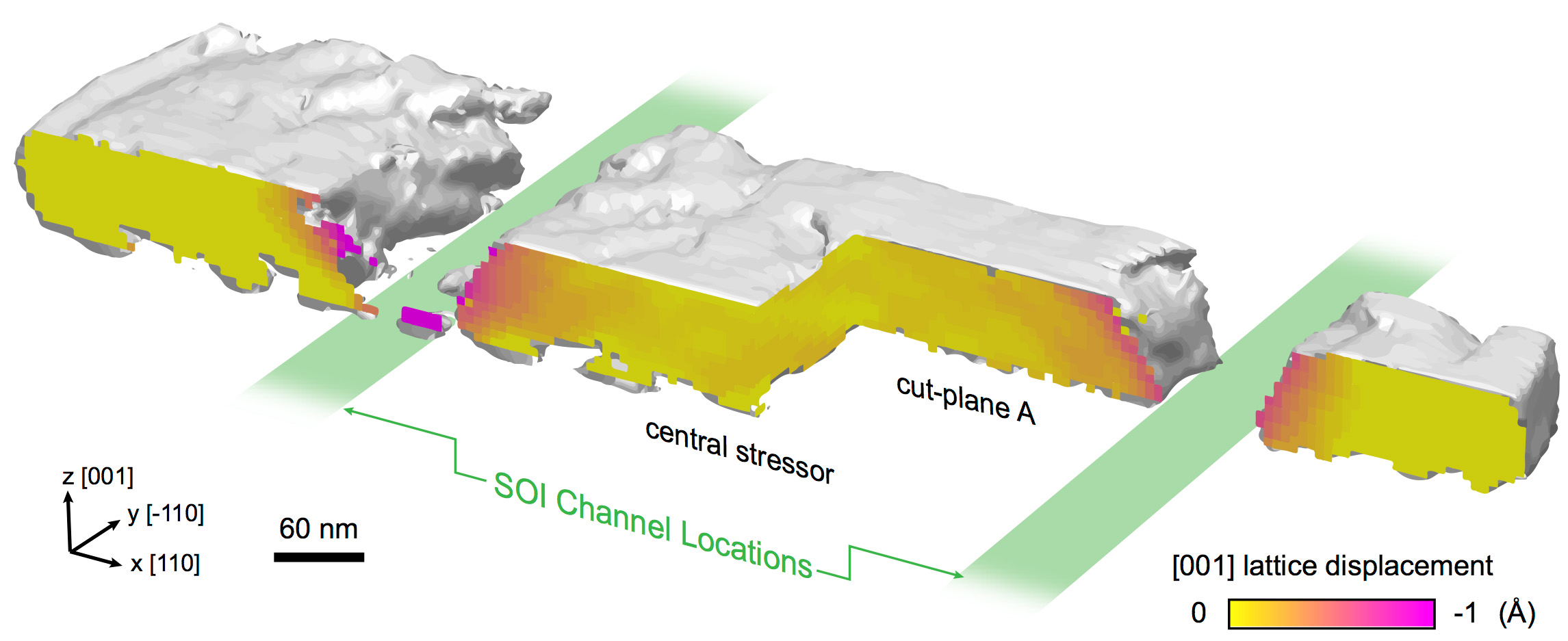
Researchers from Argonne National Laboratory, Aix-Marseille University (France), the IBM T.J. Watson Research Center, and the IBM Semiconductor Research and Development Center tested the 3DBPP technique on a prototype semiconductor device featuring lithographically-patterned silicon-germanium (SiGe) crystals. The x-ray diffraction data was gathered at the X-ray Science Division/Center for Nanoscale Materials 26-ID-C Hard X-ray Nanoprobe beamline at the APS, an Office of Science user facility at Argonne. Figure 1 shows a cutaway view of the tiny semiconductor device, revealing its morphology and internal lattice displacement, which indicates the sample's strain field.
The researchers behind this study anticipate that their 3DBPP technique will prove applicable to a variety of synchrotron beamline configurations, such as beamlines with distinct x-ray focusing setups including x-ray mirrors, diffraction gratings, or pinholes. The researchers also anticipate that 3DBPP will open up new opportunities to image materials structure in environments difficult to access with any other method, such as materials synthesis chambers, and the active regions buried deep within electronic devices.
— William Atkins and Philip Koth
See: S.O. Hruszkewycz1*, M. Allain2, M.V. Holt1, C.E. Murray3, J.R. Holt4, P.H. Fuoss1, and V. Chamard2, “High-resolution three-dimensional structural microscopy by single-angle Bragg ptychography,” Nat. Mater. 16, 244 (February 2017). DOI: 10.1038/NMAT4798
Author affiliations: 1Argonne National Laboratory, 2Aix-Marseille University, 3IBM T.J. Watson Research Center, 4IBM Semiconductor Research and Development Center
Correspondence: *shrus@anl.gov
3DBPP simulations and experimental measurements were supported by the U.S. Department of Energy (DOE) Office of Science-Basic Energy Sciences, Materials Science and Engineering Division. Design of the 3DBPP phase retrieval algorithm was partially funded by the French ANR under project number ANR-11-BS10-0005 and the French OPTITEC cluster. Use of the Center for Nanoscale Materials and the Advanced Photon Source were supported by the U.S. DOE Office of Science-Basic Energy Sciences, under Contract No. DE-AC02-06CH11357.
Argonne National Laboratory seeks solutions to pressing national problems in science and technology. The nation's first national laboratory, Argonne conducts leading-edge basic and applied scientific research in virtually every scientific discipline. Argonne researchers work closely with researchers from hundreds of companies, universities, and federal, state and municipal agencies to help them solve their specific problems, advance America's scientific leadership and prepare the nation for a better future. With employees from more than 60 nations, Argonne is managed by UChicago Argonne, LLC for the U.S. Department of Energy's Office of Science.
The U.S. Department of Energy's Office of Science is the single largest supporter of basic research in the physical sciences in the United States and is working to address some of the most pressing challenges of our time. For more information, visit the Office of Science website.