
 Additive manufacturing, also known as three-dimensional (3-D) printing, has long been used to create prototypes and is increasingly being used to build commercial items, from sneakers to aircraft parts. Most 3-D printing with metal works by scanning a laser across a thin layer of metallic powder, then melting to join with the layer below until a structure has been built up. Many such parts, however, suffer from mechanical weaknesses caused by defects in the layers, such as rough surfaces and large numbers of pores. It has been difficult to measure exactly how the defects form, in part because the process happens so quickly. Now scientists have developed a technique using the U.S. Department of Energy’s Advanced Photon Source (APS) to capture defects as they form.
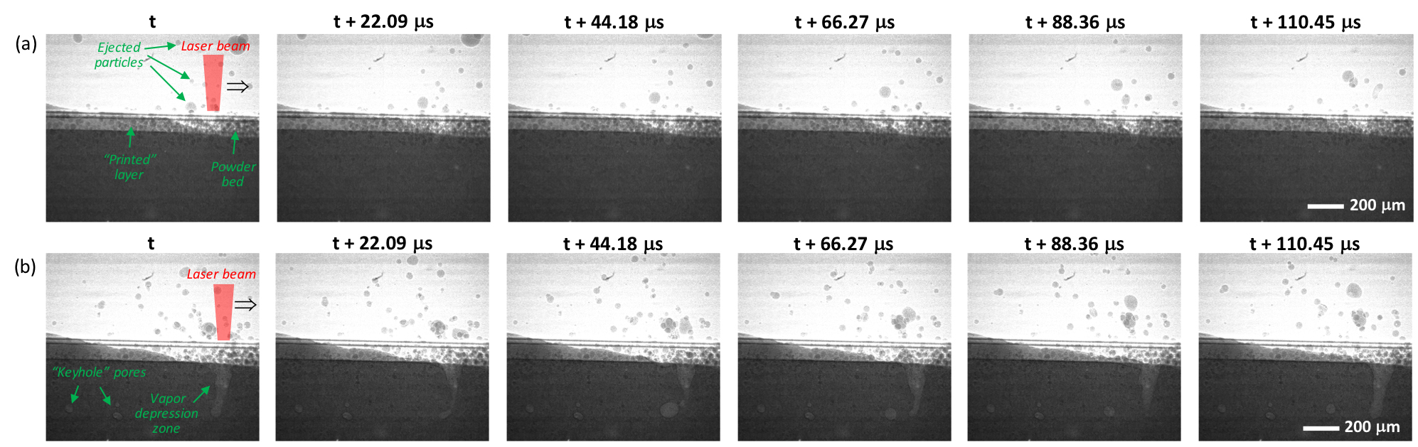
Most previous studies of the process known as “laser powder-bed fusion” had relied on high-speed photography in visible light, but that can only capture what’s happening at the surface. So the researchers from Argonne National Laboratory, Carnegie Mellon University, and the Missouri University of Science and Technology built a setup that allowed them to probe below the surface with a hard x-ray beam from the X-ray Science Division 32-ID-B,C beamline of the APS, an Office of Science user facility at Argonne. They designed and built a miniature powder bed where a laser beam from above treated the metal and they sent an x-ray beam through the molten powder bed to both an imaging and a diffraction detector.
The researchers were able to watch and measure many of the dynamics involved in the rapid heating and cooling of the metal powder, a titanium-aluminum-vanadium alloy. For instance, they observed the formation of keyhole pores, which are significant defects within the structure. When the laser struck the powder, the metal melted, and both the molten metal and the heat flowed away from the center of the zone heated by the laser (Fig. 1). When the laser was scanned away, the sample started to cool down and the metal flowed back toward the center of the melted area, but the material on the top moved more quickly than that below, resulting in a cavity in the hardened structure. The researchers measured the closure of the keyhole for the first time, and found it could be faster than 50 microseconds, too quick for trapped gas to escape before the surface closed over it.
The study also showed how the metal behaved differently at different laser power levels. When the powder was subjected to 340 watts of laser power for 1 millisecond, first the powder then the hardened metal beneath it melted and a depression was created. Eventually, a dome-shaped metal structure formed without any notable defects. But when they set the laser to 520 watts, the powder and base melted much faster, and some of the molten material was ejected, while the cavity formed was deeper. This process too produced a dome, but this one had a pore about 150 microns in diameter underneath it.
The researchers also measured such factors as the ejection rate of the material, which at high powers could be as fast as 15 meters per second. Under the conditions they used, the solidification rate of the molten alloy was about half a meter per second.
The researchers hope these kinds of measurements will improve their understanding of the processes involved in laser-bed powder fusion so that they will be able to adjust parameters such as laser power and scan speed to achieve the best microstructures. They say the technique will likely become critical in additive manufacturing, particularly as new materials and new printing processes are developed. — Neil Savage
See: Cang Zhao1, Kamel Fezzaa1, Ross W. Cunningham2, Haidan Wen1, Francesco De Carlo1, Lianyi Chen3, Anthony D. Rollett2, and Tao Sun1, “Real-time monitoring of laser powder bed fusion process using high-speed X-ray imaging and diffraction,” Sci. Rep. 7, 3602 (2017). DOI:10.1038/s41598-017-03761-2
Author affiliations: 1Argonne National Laboratory, 2Carnegie Mellon University, 3Missouri University of Science and Technology
Correspondence: *taosun@aps.anl.gov
This work is supported by Laboratory Directed Research and Development (LDRD) funding from Argonne National Laboratory, provided by the Director, Office of Science, of the U.S. Department of Energy (DOE) under Contract No. DE-AC02-06CH11357. R.C. is grateful for support from the Northrop Grumman Corporation. A.D.R. is grateful for support of the National Nuclear Security Agency under grant DE-NA0002918. LC appreciates the support from University of Missouri Research Board. This research used resources of the Advanced Photon Source, a U.S. DOE Office of Science User Facility operated for the DOE Office of Science by Argonne National Laboratory under Contract No. DE-AC02-06CH11357.
Argonne National Laboratory seeks solutions to pressing national problems in science and technology. The nation's first national laboratory, Argonne conducts leading-edge basic and applied scientific research in virtually every scientific discipline. Argonne researchers work closely with researchers from hundreds of companies, universities, and federal, state and municipal agencies to help them solve their specific problems, advance America's scientific leadership and prepare the nation for a better future. With employees from more than 60 nations, Argonne is managed by UChicago Argonne, LLC for the U.S. Department of Energy's Office of Science.
The U.S. Department of Energy's Office of Science is the single largest supporter of basic research in the physical sciences in the United States and is working to address some of the most pressing challenges of our time. For more information, visit the Office of Science website.