

Optoelectronic devices play an essential role in the modern world by converting an electric current to light (as exemplified by the ubiquitous LED lights), or conversely, by capturing light to produce electricity (as in solar cells). A class of materials offering significant potential for highly cost-effective optoelectronics are the so-called hybrid perovskites. In practice, the use of hybrid perovskites faces several challenges, including rapid changes in output in response to a voltage. Previous experiments were unable to directly observe the chemical origin of these changes. Using nanoprobe x-ray fluorescence (nano-XRF) at the U.S. Department of Energy’s (DOE's) Advanced Photon Source (APS), researchers have for the first time directly measured nanoscale changes in the chemical composition of crystals of methylammonium lead bromide, a leading hybrid perovskite candidate for optoelectronic devices. The experiments revealed how the presence of an applied voltage depleted the bromine (Br) within regions of the material, degrading its optoelectronic performance. The researchers contend that limiting bromine migration within methylammonium lead bromide, and in similar hybrid perovskites, should stabilize these compounds, thereby enhancing their outstanding optoelectronic properties and promoting their use for inexpensive, yet highly-efficient, solar cells, photonic lasers, photodetectors, and light-emitting diodes (LEDs).
To increase the practicality of solar-generated electricity, the cost of fabricating photovoltaic cells must be reduced while simultaneously boosting their power-conversion efficiency. These cost and efficiency goals have drawn researchers to study hybrid perovskites for solar cells. The methylammonium lead halide compounds exhibit exceptional optoelectronic characteristics, yet are inexpensive to manufacture. Moreover, solar conversion efficiencies of over 22% have been demonstrated in the lab using hybrid perovskite thin films.
Traditional perovskites are inorganic, oxygen-bearing minerals with distinctive octahedral within a cubic crystalline structure. Methylammonium lead bromide (chemical formula CH3NH3PbBr3) possesses the same perovskite structure with its distinctive octahedral arrangement, but differs from oxide perovskites in a couple of ways. First, the oxygen anion is replaced by bromine, one of the halogen elements (the others being iodine, chlorine, fluorine, and astatine). Second, it is an organic-inorganic compound wherein inorganic lead bromide (PbBr6) octahedra are joined with organic methylammonium cations (CH3NH3+). This organic-inorganic mixture gives the compound its excellent optoelectronic properties and leads to its designation as a “hybrid” perovskite.
Theoretical calculations indicate that hybrid perovskites possess a large number of vacancies, or missing atoms, in their crystalline structure. Theoretical considerations also indicate that certain elements within the hybrid perovskites can readily move within these vacancies when subjected to an electric potential (voltage). In the case of methylammonium lead bromide, bromine ions are by far the most likely to move in response to an applied voltage.
The techniques used in previous studies to measure halide migration exhibited various drawbacks, such as sample destruction, or imaging limited to near-surface depths. In contrast, the nano-XRF used for this study by researchers from the University of California, San Diego, AMOLF (Netherlands), and Argonne National Laboratory penetrated through the entire sample depth, while limiting damage to its crystalline structure.
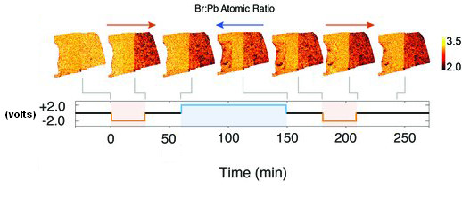
The nano-XRF measurements were made at the X-ray Science Division x-ray beamline 2-ID-D at the APS, an Office of Science user facility at Argonne. Several high-quality, thin-film crystals of methylammonium lead bromide were grown. Each rectangular crystal measured around 20 to 30 micrometers per side. Figure 1 depicts the basic experimental setup. A highly collimated x-ray beam mapped each sample's heavier elements (bromine and lead) with a parts-per-million sensitivity, in 250-nanometer steps. Following the x-ray measurements, a laser probed the same microscopic area to determine its optoelectronic response via photoluminescence. (Photoluminescence involves the absorption and reemission of light of differing wavelengths. Higher-intensity photoluminescence indicates better optoelectronic properties.) A series of x-ray and laser measurements was made while the crystal was subjected to voltages of zero, -2, and +2 volts.
Figure 2 illustrates the migration of bromine within the sample region as the voltage is varied. The images show that bromide ions move from the negative region of the sample towards the positive side. The laser-induced photoluminescence measurements demonstrated that better optoelectronic quality was associated with higher concentrations of bromine.
These findings quantitatively characterize bromine migration in methylammonium lead bromide under an applied voltage at room temperature. The findings also demonstrate that higher local bromine concentration is correlated with improved optoelectronic performance. In order to achieve the highest optoelectronic performance, the researchers suggest techniques for limiting bromine depletion in methylammonium lead bromide, such as growing the crystals in a bromine-excess environment to lower the number of crystalline vacancies following growth of the crystal. These important findings are applicable to other hybrid perovskites, such as methylammonium lead iodide wherein iodine supplants bromine. — Philip Koth
See: Yanqi Luo1, Parisa Khoram2, Sarah Brittman2, Zhuoying Zhu1, Barry Lai3, Shyue Ping Ong1, Erik C. Garnett2, and David P. Fenning1*, “Direct Observation of Halide Migration and its Effect on the Photoluminescence of Methylammonium Lead Bromide Perovskite Single Crystals,” Adv. Mater., early view publication, 1703451 (29 September 2017). DOI: 10.1002/adma.201703451
Author affiliations: 1University of California, San Diego, 2AMOLF, 3Argonne National Laboratory
Correspondence: *dfenning@eng.ucsd.edu
Y.L. acknowledges the support of the University of California (UC) Carbon Neutrality Initiative. D.P.F. acknowledges UC San Diego startup funds and the support of the Hellman Foundation. This work is part of the research program in The Netherlands Organization for Scientific Research. P.K. and E.C.G. acknowledge financial support from the European Research Council (ERC) under the European Union’s Seventh Framework Programme (FP/2007-2013)/ERC Grant Agreement No. 337328, “NanoEnabledPV.” S.B. acknowledges the grant from an industrial partnership between Philips and FOM. Z.Z. and S.P.O. acknowledge funding support from the U.S. DOE Office of Science, Basic Energy Sciences under Award No. DE-SC0012118 for the computational portion of the work as well as computing resources provided by Triton Shared Computing Cluster at the UC San Diego, the National Energy Research Scientific Computing Center, and the Extreme Science and Engineering Discovery Environment supported by the National Science Foundation under Grant No. ACI-1053575. This research used resources of the Advanced Photon Source, a U.S. DOE Office of Science User Facility operated for the DOE Office of Science by Argonne National Laboratory under Contract No. DE-AC02-06CH11357.
Argonne National Laboratory seeks solutions to pressing national problems in science and technology. The nation's first national laboratory, Argonne conducts leading-edge basic and applied scientific research in virtually every scientific discipline. Argonne researchers work closely with researchers from hundreds of companies, universities, and federal, state and municipal agencies to help them solve their specific problems, advance America's scientific leadership and prepare the nation for a better future. With employees from more than 60 nations, Argonne is managed by UChicago Argonne, LLC for the U.S. Department of Energy's Office of Science.
The U.S. Department of Energy's Office of Science is the single largest supporter of basic research in the physical sciences in the United States and is working to address some of the most pressing challenges of our time. For more information, visit the Office of Science website.