
The original American Institute of Physics (AIP) article can be read here and is © 2017 AIP Publishing LLC.
Quantum mechanics, the physics that governs nature at the atomic and subatomic scale, contains a host of new physical phenomena to explore quantum states at the nanoscale. Though tricky, there are ways to exploit these inherently fragile and sensitive systems for quantum sensing. One nascent technology in particular makes use of point defects, or single-atom misplacements, in nanoscale materials, such as diamond nanoparticles, to measure electromagnetic fields, temperature, pressure, frequency and other variables with unprecedented precision and accuracy.
Quantum sensing could revolutionize medical diagnostics, enable new drug development, improve the design of electronic devices and more.
For use in quantum sensing, the bulk nanodiamond crystal surrounding the point defect must be highly perfect. Any deviation from perfection, such as additional missing atoms, strain in the crystalline lattice of the diamond, or the presence of other impurities, will adversely affect the quantum behavior of the material. Highly perfect nanodiamonds are also quite expensive and difficult to make.
A cheaper alternative, say researchers at Argonne National Laboratory and the University of Chicago, is to take defect-ridden, low-quality, commercially manufactured diamonds, and then “heal” them.
In a paper published this week in APL Materials, from AIP Publishing, the researchers describe a method to heal diamond nanocrystals under high-temperature conditions, while visualizing the crystals in three dimensions using an x-ray imaging technique.
“Quantum sensing is based on the unique properties of certain optically active point defects in semiconductor nanostructures,” said F. Joseph Heremans, an Argonne National Laboratory staff scientist and co-author on the paper.
These defects, such as the nitrogen-vacancy (NV) centers in diamond, are created when a nitrogen atom replaces a carbon atom adjacent to a vacancy in the diamond lattice structure. They are extremely sensitive to their environment, making them useful probes of local temperatures, as well as electric and magnetic fields, with a spatial resolution more than 100 times smaller than the thickness of a human hair.
Because diamonds are biologically inert, quantum sensors based on diamond nanoparticles, which can operate at room temperature and detect several factors simultaneously, could even be placed within living cells, where they could, according to Heremans, “image systems from the inside out.”
Heremans and his colleagues, including Argonne’s Wonsuk Cha and Paul Fuoss, as well as David Awschalom of the University of Chicago, set out to map the distribution of the crystal strain in nanodiamonds and to track the healing of these imperfections by subjecting them to high temperatures, up to 800 degrees Celsius in an inert helium environment.
“Our idea of the ‘healing’ process is that gaps in the lattice are filled as the atoms move around when the crystal is heated to high temperatures, thereby improving the homogeneity of the crystal lattice,” said Stephan Hruszkewycz, also a staff scientist at Argonne and lead author on the paper.
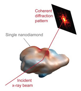
This nanodiamond healing was monitored with a three-dimensional (3-D) microscopy method called Bragg coherent diffraction imaging, performed by subjecting the crystals to a coherent x-ray beam at the X-ray Science Division 34-ID-C x-ray beamline at the U.S. Department of Energy’s Advanced Photon Source, an Office of Science user facility at Argonne. The x-ray beam that scatters off the nanodiamonds was detected and used to reconstruct the 3-D shape of the nanocrystal, “and, more importantly, the strain state of the crystal,” Hruszkewycz said.
The researchers found that nanodiamonds “shrink” during the high-temperature annealing process, and surmise that this occurs because of a phenomenon called graphitization. This phenomenon occurs when the surface of the material is converted from the normal diamond lattice arrangement into graphite, a single layer of chicken-wire-like arranged carbon atoms.
The study marks the first time that Bragg coherent diffraction imaging has been shown to be useful at such high temperatures, a capability that, Hruszkewycz said, “enables the exploration of structural changes in important nanocrystalline materials at high temperatures that are difficult to access with other microscopy techniques.”
Hruszkewycz added that the research represents “a significant step towards developing scalable methods of processing inexpensive, commercial nanodiamonds for quantum sensing and information processing.”
See: S.O. Hruszkewycz1*, W. Cha1, P. Andrich2, C.P. Anderson2, A. Ulvestad1, R. Harder1, P.H. Fuoss1, D.D. Awschalom1,2, and F.J. Heremans1,2, “In situ study of annealing-induced strain relaxation in diamond nanoparticles using Bragg coherent diffraction imaging,” APL Mat. 5, 026105 (2017). DOI: 10.1063/1.4974865
Author affiliations: 1Argonne National Laboratory, 2The University of Chicago
Correspondence: *shrus@anl.gov
BCDI measurements and sample preparation of nanocrystalline diamond were supported by the U.S. Department of Energy (DOE) Office of Science-Basic Energy Sciences, Materials Sciences and Engineering Division. Raman measurements were supported by the Air Force Office of Scientific Research and by the Army Research Office OSU-MURI (Ohio State University–Multidisciplinary University Research Initiative). C.P.A. was supported by the Department of Defense (DoD) through the National Defense Science & Engineering Graduate Fellowship (NDSEG) Program. We made use of shared Raman spectroscopy facilities supported by the NSF MRSEC Program under DMR- 0820054. This research used resources of the Advanced Photon Source, a U.S. DOE Office of Science User Facility operated for the DOE Office of Science by Argonne National Laboratory under Contract No. DE-AC02- 06CH11357.
APS home page image for this article from S.O. Hruszkewycz et al., APL Mat. 5, 026105 (2017). © 2017 AIP Publishing LLC.
Argonne National Laboratory seeks solutions to pressing national problems in science and technology. The nation's first national laboratory, Argonne conducts leading-edge basic and applied scientific research in virtually every scientific discipline. Argonne researchers work closely with researchers from hundreds of companies, universities, and federal, state and municipal agencies to help them solve their specific problems, advance America's scientific leadership and prepare the nation for a better future. With employees from more than 60 nations, Argonne is managed by UChicago Argonne, LLC for the U.S. Department of Energy's Office of Science.
The U.S. Department of Energy's Office of Science is the single largest supporter of basic research in the physical sciences in the United States and is working to address some of the most pressing challenges of our time. For more information, visit the Office of Science website.