
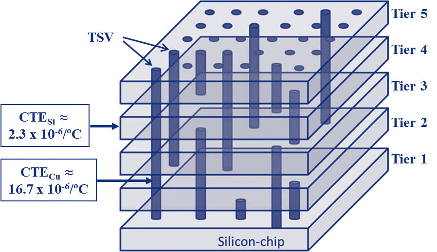
In the past, microelectronics were essentially a two-dimensional affair based upon flat integrated circuit chips connected to each other. Then, engineers opened up the third dimension, with integrated circuit chips stacked one atop another and joined electrically by vertical copper interconnects called through-silicon vias (TSVs) that passed completely through the silicon wafers. But while such TSV technology allows denser circuit design with higher performance, it also increases susceptibility to the inevitable thermal fatigue that occurs in any physical system repeatedly subjected to fluctuating temperature extremes.
To understand how thermal cycling leads to mechanical stresses and failure in TSVs, a team of investigators from the National Institute of Standards and Technology, Argonne National Laboratory, and SEMATECH examined copper (Cu) TSVs with synchrotron-based x-ray micro-diffraction experiments carried out at the U.S. Department of Energy’s Advanced Photon Source.
Their work provides an important and previously unavailable in situ perspective into the fundamental effects of thermal cycling in copper TSVs. Based on these experiments, the investigators suggest that currently employed "keep-out zone" design rules should be modified to account for the observed evolution of these thermally-induced stresses over time, instead of merely accounting for only the static stresses present in newly-fabricated Cu TSVs.
While some previous studies have examined the reliability of Cu TSV interconnects after thermal cycling, no work had been published that experimentally related the built-up stresses (which are the underlying cause of failure in Cu TSVs) with the witnessed number of thermal cycles.
In this experiment, the researchers examined and compared Cu TSVs in an "as received" state (new and unused, without any thermal cycling except during the manufacturing process) with identical TSVs subjected to 1000 thermal cycles.
By the use of their previously demonstrated measurement procedure, which includes the use of a depth-profiler and three optimally positioned area detectors, the investigators achieved in situ determination of the full strain and stress tensors as a function of TSV depth.
Samples were studied at the X-ray Science Division 34-ID-E x-ray beamline of the Argonne Advanced Photon Source, an Office of Science user facility. The team subjected one TSV to thermal cycling that involved repeated heating and cooling from 30˚ C to 150˚ C. The x-ray micro-diffraction instrument on the 34-ID-E beamline provided depth-dependent data for stress characterization, along with information on lattice and crystallographic structure.
The stresses in the as-received Cu TSV sample were quite low, although they fluctuated somewhat along the TSV depth. The mean absolute hydrostatic stress in the sample was measured at 16 ± 44 MPa, a value attributed to stress relaxation resulting from storage at room temperature for nine months.
The TSV subjected to 1000 thermal cycles also displayed significant fluctuations in stress along its depth. However, the stresses were significantly greater, measuring an average of eight times higher at 123 ± 37 MPa. Significant differences were also measured in shear stresses between the as-received sample and the cycled TSV at different depths.
The as-received TSV showed a mean absolute shear stress of 28 ± 20 MPa with a maximum of 73 ± 19 MPa at a 32.5-µm depth, while the cycled TSV demonstrated a maximum shear stress of -118 ± 18 MPa at 22.5-µm depth, and a mean absolute shear stress of approximately 34 MPa. Differences in grain orientation coupled with the variation in the confinement of the TSV resulted in the depth-dependent stress fluctuations measured in both the as-received and cycled TSV samples.
The researchers cite strain hardening resulting from the entanglement of dislocations as the cause of the much higher stresses observed in the 1000-cycled TSV sample, which measured 353 ± 21 MPa at their maximum value in the center of the TSV.
The continued increase in dislocation density and entanglement caused by repeated thermal cycling will eventually lead to the formation of defects such as microscopic cracks and voids, which can result in structural weakness and failure as damage continues to accumulate. These researchers note that such repeated thermal cycling and damage in Cu TSVs will adversely affect the performance and lifespan of neighboring front-end-of-line devices.
— Mark Wolverton
See: Chukwudi Okoro1, Lyle E. Levine1, Ruqing Xu2, Klaus Hummler3, and Yaw Obeng1, "Synchrotron-based measurement of the impact of thermal cycling on the evolution of stresses in Cu through-silicon vias," J. Appl. Phys. 115, 243509 (2014). DOI:10.1063/1.4885461]
Author affiliations: 1National Institute of Standards and Technology, 2Argonne National Laboratory, 3SEMATECH
Correspondence: * chukwudi.okoro@nist.gov
This research used resources of the Advanced Photon Source, a U.S. Department of Energy Office of Science User Facility operated for the DOE Office of Science by Argonne National Laboratory under Contract No. DE-AC02-06CH11357.
Argonne National Laboratory is supported by the Office of Science of the U.S. Department of Energy. The Office of Science is the single largest supporter of basic research in the physical sciences in the United States, and is working to address some of the most pressing challenges of our time. For more information, please visit science.energy.gov.