
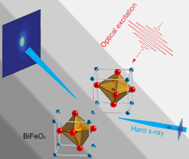
Multiferroics are in a class of materials that exhibits more than one ferroic order simultaneously. One of the prototypical multiferroics is BiFeO3, an important material because it is one of a few materials that exhibit both ferroelectricity and magnetism at room temperature. The interaction of BiFeO3with light has attracted great attention because optical control of either magnetism, ferroelectricity, or both has implications for future electronic devices.
The origin of a large photoexcited structural change in BiFeO3was not well understood because of the lack of direct experimental evidence, preventing a rational design for future optomechanical and optoelectrical applications using ferroelectric and multiferroic materials.
Now, a team of researchers led by Argonne scientists at the Advanced Photon Source (APS) and Center for Nanoscale Materials (CNM), along with colleagues from the University of Wisconsin-Madison, Cornell University, Northwestern University, Sandia National Laboratories, and Kavli Institute at Cornell for Nanoscale Science, has revealed the electronic origin of the interaction between lattice structure and optical light using a nanometer-thick layer of BFO at the atomic level and ultrafast time scales. Their work was recently published in Physical Review Letters.
Under illumination with light, these multiferroic respond by creating a large electric current, termed a photocurrent, and can also change their atomic structure, both of which are potentially useful in applications.
“One of the central problems is how the physical processes associated with the absorption of light in multiferroics leads to these potentially useful properties,” said Paul Evans, an article co-author and professor at the University of Wisconsin-Madison.
Utilizing state-of-art tools readily available at Argonne, a new approach was employed to study what happens after BiFeO3 is excited by an intense pulse of light. Structural studies were conducted using the X-ray Science Division (XSD) 7-ID-C ultrafast x-ray diffraction beamline at the APS. These structural results were compared with the electronic response measured at the ultrafast spectroscopy lab led by Richard Schaller at the CNM.
“The large, optically induced strain decays within several billionths of a second, which turned out to be the same rate as the excited electrons return to their initial state,” said Haidan Wen, the lead author of the paper and an assistant physicist with XSD. This key insight showed that the structural rearrangements after optical excitation were largely driven by electronic processes.
Faster data storage devices with lower power consumption can result from optical control of electronic and structural properties. This understanding of how that light can induce simultaneous structural and electronic effects now enables optical control of ferroelectric and multiferroic materials without requiring electrical contacts.
According to John Freeland, a co-author and a physicist in XSD, “The large optically induced strain opens a new route for ultrafast strain engineering of multifunctional complex oxides and new opportunities for manipulation of magnetism for spintronic applications.”
The researchers also believe that the technique can be applied to many other complex material systems and can be helped dramatically by the APS Upgrade. The development over the next five years of a short-pulse x-ray source at the APS will shorten the x-ray pulse by about a factor of 50.
“Then we will see more detail of the electrons and atoms in action, and probe physics that is out of reach now, especially these occurring in the material right after the excitation by the laser pulse,” said Yuelin Li, an XSD physicist and the paper’s corresponding author.
See: Haidan Wen1, Pice Chen2, Margaret P. Cosgriff2, Donald A. Walko1, June Hyuk Lee1, Carolina Adamo3, Richard D. Schaller1,4, Jon F. Ihlefeld5, Eric M. Dufresne1, Darrell G. Schlom3,6, Paul G. Evans2, John W. Freeland1, and Yuelin Li1*, “Electronic Origin of Ultrafast Photoinduced Strain in BiFeO3,” Phys. Rev. Lett. 110, 037601 (2013). DOI: 10.1103/PhysRevLett.110.037601
Author affiliations: 1Argonne National Laboratory, 2University of Wisconsin–Madison, 3Cornell University, 4Northwestern University, 5Sandia National Laboratories, 6Kavli Institute at Cornell for Nanoscale Science
Correspondence: *ylli@aps.anl.gov
Work at Argonne was supported by the U.S Department of Energy, Office of Science under Contract No. DE-AC02-06CH11357.
The Advanced Photon Source at Argonne National Laboratory is one of five national synchrotron radiation light sources supported by the U.S. Department of Energy’s Office of Science to carry out applied and basic research to understand, predict, and ultimately control matter and energy at the electronic, atomic, and molecular levels, provide the foundations for new energy technologies, and support DOE missions in energy, environment, and national security. To learn more about the Office of Science x-ray user facilities, visit http://science.energy.gov/user-facilities/basic-energy-sciences/.
Argonne National Laboratory seeks solutions to pressing national problems in science and technology. The nation's first national laboratory, Argonne conducts leading-edge basic and applied scientific research in virtually every scientific discipline. Argonne researchers work closely with researchers from hundreds of companies, universities, and federal, state and municipal agencies to help them solve their specific problems, advance America's scientific leadership and prepare the nation for a better future. With employees from more than 60 nations, Argonne is managed by UChicago Argonne, LLC for the U.S. Department of Energy's Office of Science.