
A newly dedicated beamline at the U.S. Department of Energy’s Advanced Photon Source can shed light on the fundamental physics that govern ordering in block copolymer systems. Understanding these physical principles is critical for practical applications of block copolymer lithography. For example, perfect positioning of domains is necessary to pattern high-density disk drives, because each block copolymer domain defines the location of a “bit” (data storage unit) that needs to be individually addressed. The researchers who carried out the work are currently studying whether or not the vibration modes responsible for the less perfect positional order can be eliminated.
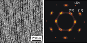
Self-assembly of block copolymers is widely investigated as a simple, inexpensive route for patterning high-density arrays of nanoscale features. The simplest block copolymer architecture is the diblock, which is constructed by chemically linking two different types of polymer chains at their ends. The immiscibility between unlike segments drives them to self-assemble into periodic domains, a process termed “micro-phase separation.” The resulting morphology (such as lamellar sheets, cylinders, or spheres) is largely determined by the copolymer composition, while domain size and periodicity are controlled by the length of the polymer chains, and are on the order of 10 nm. This length scale is well below the limits of conventional optical lithography, the technique employed by the semiconductor industry to define features in integrated circuits, for example. In optical lithography, a thin polymeric film (“resist”) is exposed to light through a mask. The solubility of the exposed regions is changed, and the pattern is then “developed” in a solution that only removes the soluble regions. Block copolymer lithography uses chemistry to selectively remove one component. However, the substrate (a silicon wafer, for example) must have features that control the positioning of domains. Furthermore, assessing the quality of the domain placement over the entire wafer is extremely challenging due to the small feature size. While high-resolution microscopy can resolve individual block copolymer domains, this technique is limited to extremely small sampling areas (~10-6 mm2).
Researchers from Professor Edward Kramer’s group of the University of California in Santa Barbara have patterned single crystals of 10-nm block copolymer spheres across an entire 2-in.-diameter silicon wafer. The silicon wafer was first patterned with photolithography to produce 12-µm-wide hexagonal wells. A single layer of block copolymer spheres was then self-assembled inside the wells. Together with Argonne researchers, the group used grazing-incidence small-angle x-ray scattering (GISAXS) or diffraction to measure the crystal quality over macroscopic areas (~2 mm2 per measurement) on the X-ray Operations and Research 8-ID beamline at the Advanced Photon Source, where a dedicated GISAXS beamline has been constructed to serve the nanoscience user community. As an increasingly important structural-characterization technique, GISAXS is ideally suited for studying structure and morphology in nanostructures and nanocomposites at surfaces and interfaces.
In this experiment, it was found that the orientation of the crystallographic planes was nearly perfect, demonstrating that single crystals resulted in each well. This was confirmed with high-resolution microscopy measurements. However, the positional correlation function extracted from the diffraction data demonstrated algebraically decaying order, meaning the position of each sphere was not locked into a perfect hexagonal grid. Such behavior has been predicted theoretically for two-dimensional hexagonal arrays, and results from thermally induced “lattice vibrations.” The results were published in Phys. Rev. Lett. 98, 086101 (2007) and featured on the journal cover.
Contact: Edward Kramer edkramer@mrl.ucsb.edu
See: G. E. Stein, E. J. Kramer, X. Li, and J. Wang, “Single-Crystal Diffraction from Two-Dimensional Block Copolymer Arrays,” Phys. Rev. Lett. 98, 086101 (2007). doi:10.1103/PhysRevLett.98.086101
This work was supported by the NSF DMR Polymers program Grant No. DMR0307233. This work benefited from use of the UCSB MRL facilities, which is supported by the MRSEC program of the NSF under Grant No. DMR05-20415, and from use of the UCSB nanofabrication facilities, which is supported by the NSF-NNIN under Grant No. 44772-7475. Use of the APS was supported by the U.S. DOE, Office of Science, Office of Basic Energy Sciences, under Contract No. DE-AC02-06CH11357.
Argonne is a U.S. Department of Energy laboratory managed by UChicago Argonne, LLC