
Most thin films grow on substrates in only three ways: layer by layer, formation of atomic islands, or layers followed by islands. The particular growth mode that a given material will follow crucially depends on the relative magnitudes of the surface energy of the film versus the interfacial energy of the film on the substrate. Recently, a team of researchers from the University of Illinois, Academica Sinica in Taiwan, Georgia Tech, and the City University of Hong Kong has discovered a remarkable anomaly. By means of real-time x-ray scattering measurements, the researchers found that lead films grown on silicon adopt a completely novel pattern of growth.
Earlier studies of lead films on silicon with scanning tunneling microscopy and electron diffraction revealed hints that certain island heights above the substrate were preferred over others. These "magic" dimensions suggest that quantum size effects play a strong role in the formation of the films. Yet, the magic numbers do not seem to bear any relation to characteristic dimensions or length scales of the films themselves. In order to unravel this puzzle, the researchers also performed first-principles density functional calculations to understand their experimental results.
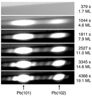
Real-time x-ray scattering measurements of the film structure were obtained with a growth chamber placed at UNI-CAT beamline 33-ID at the APS. Lead vapor from an effusion cell was deposited at a rate of 0.0044 monolayers per second onto silicon substrates prepared to expose the (111)-7X7 surface. A CCD camera captured the scattered 26.05-keV x-rays from the APS undulator beam (Fig. 1) in order to measure reflectivity and truncation rod scattering at regular intervals. Film growth was monitored in situ with a vibrating quartz thickness gauge and the temperature of the sample was monitored with a thermocouple.
Truncation rod profiles obtain-ed from the CCD images give a detailed picture of the film evolution during growth. From the interference fringes, information about island height and film thickness is deduced. At first, there is an increase in the intensity of the silicon surface diffraction, indicating that a lead wetting layer is forming, commensurate with the underlying substrate lattice. After a thickness of about 1.1 monolayer, the silicon diffraction intensity decreases, followed by a rise in lead intensity and island formation at a deposition of 1.5 monolayer. At this stage, the islands begin growing up to a height of 5 monolayers above the wetting layer (a net island height of 6 monolayers). Then, in an unusual departure from typical growth modes, the islands remain locked at this height but begin growing horizontally until all of the islands have filled in to form a single 6-monolayer film. Now the growth switches completely from island growth to layer-by-layer growth for the rest of the film's evolution.
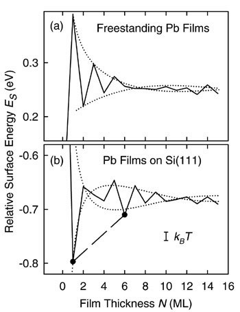
Two characteristic thicknesses emerge from this analysis: the one-monolayer wetting layer, which gives way to island formation, and the 6-monolayer magic island height. To make sense of these critical thicknesses, the researchers performed first-principles calculations of the relative surface energy per surface atom of the films (Fig. 2). For free-standing lead films, the energy follows a typical damped Friedel oscillation pattern with a period of 1.8 monolayer. When the calculation is done for lead atoms on a silicon substrate, however, the altered boundary condition produces a phase shift in the envelope function, resulting in deep minima at 1 monolayer and 6 monolayers.
The absolute energy minimum at 1 monolayer explains the wetting layer, while the minimum at 6 monolayers accounts for the magic island height. For coverages between these two values, the system would be expected to phase separate into a linear combination of the two, in excellent agreement with the behavior observed in the island formation. As shown by this work, taking into the consideration the global energy picture and not just the local energy landscape is essential in understanding the complete story of thin-film growth.
See: H. Hong, C.-M. Wei, M.Y. Chou, Z. Wu, L. Basile, H. Chen, M. Holt, and T.-C. Chiang, Phys. Rev. Lett 90(7), 076104-1 to 076104-4 (21 February 2003).
This work was supported by the U.S. Department of Energy (Grants No. DEFG02-91ER45439 and No. DEFG02-97ER45632), the R.O.C. National Science Council (Grant No. 90-2112-M-001-062), the U.S. National Science Foundation (Grants No. DMR-02-03003 and No. SBE-01-23532), and the Petroleum Research Fund administered by the American Chemical Society. The UNI-CAT facility at the APS is supported by the University of Illinois Frederick Seitz Materials Research Laboratory (U.S. Department of Energy and the State of Illinois-IBHEHECA), the Oak Ridge National Laboratory (U.S. Department of Energy under contract with Lockheed Martin Energy Research), the National Institute of Standards and Technology (U.S. Department of Commerce), and UOP LLC. The APS is supported by the U.S. Department of Energy (Grant No. W-31-109-ENG-38).