The list of potential mechanisms that underlie an unusual metal-insulator transition has been narrowed by a team of scientists using a combination of x-ray techniques at the U.S. Department of Energy’s Advanced Photon Source (APS). This transition has ramifications for materials design for new and improved electronics and sensors.
The transition between being electrically conductive (metallic) at high temperatures and electrically insulating at lower temperatures is known as a metal-insulator transition (MIT). Pinpointing the activation mechanism that allows crystals used in devices such as transistors in electronics and temperature-based sensor control systems used in manufacturing to change their electrical state is key to developing new devices that are smaller and more efficient than those in use today.
For example, transistors — and most electronics — function by tuning conductivity, essentially using the level of electrical resistance as an on-off switch or as a sensor. Designing new electronic devices has been largely driven by trial and error. Understanding what causes large changes in electrical conductivity, as in an MIT, can permit the design of new materials that are cheaper or have higher-performance properties.
The team of researchers from the Argonne and Lawrence Berkeley national laboratories, the University of Illinois at Chicago, and the University of Arkansas made inroads in understanding this transition by using the Argonne APS, an Office of Science user facility, to study rare-earth crystal family perovskites, in particular the rare-earth atom compounds nickelates. These are compounds that contain a central nickel atom bonded to oxygen or oxygen-containing groups and are considered an ideal model for the study of this transition.
The team studied thin films of neodymium nickel oxide (NdNiO3), using three different beamlines at the APS, which allowed an in-depth exploration of the samples. Resonant inelastic x-ray scattering (RIXS) was done at the X-ray Science Division (XSD) 9-ID-B beamline RIXS end station (which has been recently incorporated into the Sector 27 RIXS beamline); x-ray absorption spectroscopy was performed at XSD beamline 4-ID-D; and resonant x-ray diffraction was performed at XSD beamline 6-ID-B.
Nickelates are considered an ideal model for studying the transition because they display strongly correlated electronic behavior that gives rise to unique electronic and magnetic properties. Several competing theories exist to explain the mechanics that drive the transition but none satisfy all the experimental findings. The team was able to rule out some of those theories. The results were published in Physical Review Letters.
APS beamlines provide the high photon flux and energy that are critical when dealing with subtle electronic effects. State-of-the-art optics and collaboration between beamlines allows unparalleled detail in the study of materials. The application of the RIXS technique to a long-standing problem was made possible by improved capabilities in thin-film measurements at the beamline.
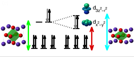
To study the transition, chemically identical film samples were grown with small structural distortions induced by epitaxial strain. Slight differences in lattice constants brought about substantial changes in electronic behavior. A film with a tensile distortion, where all the atoms are more distant from each other, exhibits the electrical transition. A film grown with a slightly compressive distortion, where all atoms are brought closer together, is electrically conductive at all temperatures.
The measurements suggest that tensile strain facilitates the transfer of electrons between two elementally different atoms. This observation was a surprise because the atoms in question had been assumed to be isolated from each other. These results strongly suggest a need to re-examine other, similar state transitions in perovskites. This transition is neither a pure Mott-Hubbard transition, despite electron localization, nor a simple charge-transfer transition.
See: M. H. Upton1*, Yongseong Choi1, Hyowon Park2,1, Jian Liu3, D. Meyers4, J. Chakhalian4, S. Middey4, Jong-Woo Kim1, and Philip J. Ryan1**, “Novel Electronic Behavior Driving NdNiO3 Metal-Insulator Transition,” Phys. Rev. Lett. 115, 036401 (17 July 2015). DOI: 10.1103/PhysRevLett.115.036401
Author affiliations: 1Argonne National Laboratory, 2University of Illinois at Chicago, 3Lawrence Berkeley National Laboratory, 4University of Arkansas
Correspondence: *mhupton@aps.anl.gov, **pryan@aps.anl.gov
Work at the Advanced Photon Source is supported by the U.S. Department of Energy (DOE) Office of Science under Grant No. DEAC02-06CH11357. J.C., D.M., and S.M. were supported by Department of Defense-Army Research Office under the Grant No. 0402-17291. H. Park gratefully acknowledges the support of start-up funds from the University of Illinois at Chicago and Argonne. This research used resources of the Advanced Photon Source, a U.S. DOE Office of Science User Facility operated for the DOE Office of Science by Argonne National Laboratory under contract no. DE-AC02-06CH11357.
Argonne National Laboratory is supported by the Office of Science of the U.S. Department of Energy. The Office of Science is the single largest supporter of basic research in the physical sciences in the United States, and is working to address some of the most pressing challenges of our time. For more information, please visit science.energy.gov.